Sign up for the Design News Daily newsletter.
Researchers at the University of Buffalo have developed a nanocavity to potentially improve the design of ultrathin solar panels, video cameras, and other optoelectronic devices.
Elizabeth Montalbano
June 28, 2016
3 Min Read
.svg?width=850&auto=webp&quality=95&format=jpg&disable=upscale "Nanocavity Paves Way for Thinner Solar Panels, Optoelectronic Devices")
Researchers have been looking for ways to improve energy absorption and transfer to improve photovoltaics and optoelectronics. We told you recently how scientists invented new energy-carrying particles to this end, and now researchers at the University of Buffalo (UB) are experimenting with nanotechnology to improve the design of ultrathin solar panels, video cameras, and other optoelectronic devices.
A team led by Qiaoqiang Gan, assistant professor of electrical engineeringat UB’s School of Engineering and Applied Sciences, has developed an optical nanocavity made, from top to bottom, of molybdenum disulfide (MoS), aluminum oxide, and aluminum. MoS is a two-dimensional semiconductor commonly used in lubricants and steel alloys that has a bandgap structure similar to semiconductors used in LEDs, lasers, and solar cells.
A nanocavity, meanwhile, is an arrangement of mirrors that allows beams of light to circulate in closed paths. These cavities are used to help build things like lasers and optical fibers used for communications.
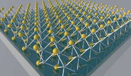
Researchers at the University at Buffalo have developed an optical nanocavity made, from top to bottom, of molybdenum disulfide (MoS2), aluminum oxide, and aluminum.
(Source: University at Buffalo)
The team’s work with the nanocavity aims to solve an issue currently in demand to manufacture smaller, thinner, and more powerful optoelectronic devices. These devices also have smaller semiconductors, which do not absorb light as well as conventional bulk semiconductors. Makers of these products must sacrifice optical absorption capacity for a thinner form factor, said Haomin Song, an electrical engineering student who worked on the project with Gan.
“Industry has kept pace with the demand for smaller, thinner, and more powerful optoelectronic devices, in part, by shrinking the size of the semiconductors used in these devices,” Song explained. “A problem for energy-harvesting optoelectronic devices, however, is that these ultrathin semiconductors do not absorb light as well as conventional bulk semiconductors. Therefore, there is an intrinsic trade-off between the ultrathin semiconductors’ optical absorption capacity and their thickness.”
The nano cavity -- which engineers coated with a single layer of MoS molecules -- could potentially solve this issue and improve optical absorption even in thinner semiconductors, Gan said. This is because it can increase the amount of light that ultrathin semiconducting materials absorb.
READ MORE ARTICLES ON SOLAR ENERGY RESEARCH:
Indeed, in experiments, the nanocavity was able to absorb nearly 70% of the laser that researchers projected onto it. Its ability to absorb light and convert that light into available energy could help in the development of more efficient and flexible solar panels, as well as faster photodetectors for video cameras and other devices, Gan said. “It may even be used to produce hydrogen fuel through water splitting more efficiently,” he added.
Gan and the team published a paper about their work in the journal, 2D Materials. Grants from the National Science Foundation, the US Army Research Office, and the US Air Force Office of Scientific Research supported the research.
The team will continue their work, experimenting with the nanocavity to reduce the energy demand and increase the energy-harvesting efficiency. “We are trying to develop applications that require stronger light–matter interaction including LEDs, solar cells, phototransistors, surface photocatalysis, and sensors,” Song said. “We are currently working on the atomically thin photodetector/photovoltaic device based on this nanocavity concept.”
Elizabeth Montalbano is a freelance writer who has written about technology and culture for more than 15 years. She has lived and worked as a professional journalist in Phoenix, San Francisco and New York City. In her free time she enjoys surfing, traveling, music, yoga and cooking. She currently resides in a village on the southwest coast of Portugal.
About the Author(s)
You May Also Like
Editors' Choice


Jun 4 - Jun 6, 2024
Jun 4 - Jun 6, 2024
Innovation in automation starts here. Discover and collaborate on automation solutions that are revolutionizing the entire production lifecycle — from design to production to market — and sharpen your competitive edge. ATX South is part of IME South, a six-in-one expo offering the latest insights & solutions spanning medtech, packaging, automation, plastics, design, & processing.
Register Now