Embedding Sensors on Chips Could Answer AIoT Needs
Sensor startup uses modified MEMS approach to produce ICs with integrated sensors that could lower costs and allow more flexible designs.

As the AIoT (Artificial Intelligence of Things) market grows, the need for sensors to monitor conditions and collect data becomes more important. But one hurdle has been the ability to easily mass produce sensors. A British sensor startup company, Nanusens, believes it has developed a solution.
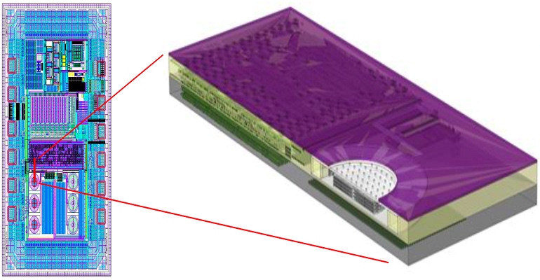
Nanusens’ technology creates the sensors directly within the control chip of the device, or ASIC, as the chip is being manufactured. This arrangement enables the sensors to occupy an insignificant amount of space by being in the chip itself, rather than taking up space by being packaged beside it. The technology also allows many different sensors to be built into a chip, thus enabling chip manufacturers and OEMs to make much smarter devices with a negligible increase in costs or space taken up inside the device. The multi-sensor solution potentially frees up space for more features and larger batteries to give a longer device life with lower power consumption.
By contrast, current sensor manufacturing builds sensors on a tiny sliver of silicon, or die, by specialized companies with each sensor type being produced on a dedicated production line, making it more difficult to ramp up production. These are either packaged into the familiar black unit with wire connections to be mounted on a PCB or fixed beside the main chip as a bare die. Both approaches are relatively expensive and large with no current way to reduce costs and size, forming a barrier to the advancement of AIoT.
Nanusens was able to use MEMS (microelectromechanical systems) technology to fabricate the sensors. “We have added a very simple post-processing step, vapor HF, to remove part of the silicon oxide of the back-end of the CMOS, releasing part of the metal layers in the back-end of the chip, so that they can move,” said Dr. Josep Montanyà, CEO of Nausens, in an e-mail interview with Design News. “The big difficulty has been in how to design these MEMS, that were to be manufactured using metal lines with bad mechanical properties (thin and with large residual stress).”
The company also developed a control circuit that measures the capacitance changes within the sensor to provide sensor data. Like the sensor itself, this is also a digital IP block so it can be incorporated in the floor plan of the device’s control chip, or ASIC, using standard EDA tools. According to Nanusens, this pairing of sensors and control circuitry as IP is unique as no other sensor solution can be turned into an IP block and made using standard CMOS techniques within the layers of the chip structure. The company believes this approach reduces the complexity and bill of materials costs for an AIoT device.
Nanusens’ Dr. Montanyà cites the benefits of the technology being lower cost, smaller size, high volume production capability, and lower current consumption in lower nodes. “The cost of the sensor is lower, because you don’t need a separate package, and it is a very small part of the main processor chip,” he said. “Not only it is monolithically integrated, but it is also very small. And smaller with lower nodes.
According to Dr. Montanyà, Nanusens has an agreement with Azoteq to develop a multi-sensor IC integrating Nanusens’ 3D accelerometer in the market by the end of next year. The company is also engaged in talks with several other semiconductor companies for more IP deals. Nanusens has already started a Series A funding round.
Besides accelerometer sensors, Nanusens is developing other types of embedded sensors such as gyroscopes, magnetometers, pressure sensors, microphones, IR imagers and gas sensors as variants on the accelerometer design. This could open up many other markets for embedded sensors such as smartphones, earbuds, wearables, automotive, medical equipment and aerospace, among other markets.
Spencer Chin is a Senior Editor for Design News covering the electronics beat. He has many years of experience covering developments in components, semiconductors, subsystems, power, and other facets of electronics from both a business/supply-chain and technology perspective. He can be reached at [email protected]
|
About the Author(s)
You May Also Like


