Heated AI Chip Battle Reaches Fever Pitch
Meta, Google, and Intel unveil new chips to handle ever-larger AI workloads.

At a Glance
- Meta unveils latest version of its Training and Inference Accelerator chip for AI infrastructure.
- Google introduced a tensor processing unit (TPU) and Arm-based CPU.
- Intel introduced its Gaudi 3 accelerator to bring generative AI to enterprises.
The race to develop faster and more powerful chips for AI and machine learning intensified this week as a company better known for its social media technology and controversial leader─Meta─has fired the latest salvo.
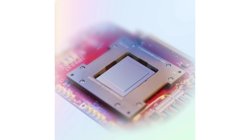
A blog post on Meta’s site Wednesday revealed the company has unveiled the second generation of its Training and Inference Accelerator, a chip intended to power the company’s AI infrastructure. Meta introduced the first version of this chip last year, and is touting performance improvements in the second-generation part.
Unlike chipmakers Intel and Nvidia, which in recent months have headlocked in a battle to produce faster and more powerful processors for AI and high-end computing, Meta is not aiming at the mass market AI customers with its part. But the company has chosen the custom silicon path to meet its own AI processing needs.
Inside Meta’s Accelerator
According to Meta, the accelerator comprises an 8x8 grid of processing elements (PEs). These elements provide significantly increased dense compute performance (3.5x over the predecessor MTIA v1) and sparse compute performance (7x improvement). Meta says these improvements stem from enhancing the architecture associated with pipelining of sparse compute.
Meta also tripled the size of the local PE storage, doubled the on-chip SRAM from 64 to 128 MB, increased its bandwidth by 3.5X, and doubled the capacity of LPDDR5. The new chip runs at a clock rate of 1.35 GHz, up from 800 MHz previously. Meta built its new chip, which is physically larger than its predecessor, with a 5-nm rather than 7-nm process.
To support the next-generation silicon, Meta developed a large, rack-based system that holds up to 72 accelerators. This system comprises three chassis, each containing 12 boards that house two accelerators each. The configuration ensures the ability to accommodate higher compute, memory bandwidth, and memory capacity.
On the software end, Meta said in its blog it further optimized its software stack to create the Triton-MTIA compiler backend to generate the high-performance code for the MTIA hardware. The Triton-MTIA backend performs optimizations to maximize hardware utilization and support high-performance kernels.
Google’s In-House Effort
Like Meta, Google is going in-house with custom silicon for its AI development. During the company’s Cloud Next computing event Tuesday, Google reportedly released details of a few version of its AI chip for data centers, as well as announcing an Arm-based central processor. The tensor processing unit (TPU), which Google is not selling directly but is available to developers through Google Cloud, reported can achieve twice the performance of Google’s previous TPUs.
Google’s new Arm-based central processing unit (CPU), called Axion, reportedly offers better performance than x86 chips. Google will also offer Axion through via Google Cloud.
Don’t Forget Intel
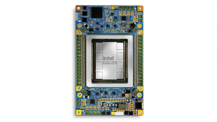
Not to be left out, Intel earlier this week revealed its Gaudi 3 AI accelerator during the company’s Intel Vision event. Gaudi 3 is designed to deliver four times faster AI computing, provide a 1.5x increase in memory bandwidth, and double the networking bandwidth for massive system scale-out compared to its predecessor.
Intel expects the chip to significantly improve performance and productivity for AI training and inference on popular large language models (LLMs) and multimodal models.
The Intel Gaudi 3 accelerator is manufactured on a 5 nanometer (nm) process and is designed to allow activation of all engines in parallel — with the Matrix Multiplication Engine (MME), Tensor Processor Cores (TPCs), and Networking Interface Cards (NICs) — enabling the acceleration needed for fast, efficient deep learning computation and scale.

Intel's Gaudi 3 accelerator. (Intel)
Key features of Gaudi 3 include:
AI-Dedicated Compute Engine: Each Intel Gaudi 3 MME can perform an impressive 64,000 parallel operations, allowing a high degree of computational efficiency, enabling them to handle complex matrix operations, a type of computation fundamental to deep learning algorithms.
Memory Boost for LLM Capacity Requirements: 128 gigabytes (GB) of HBMe2 memory capacity, 3.7 terabytes (TB) of memory bandwidth, and 96 megabytes (MB) of on-board static random access memory (SRAM) provide ample memory for processing large GenAI datasets on fewer Intel Gaudi 3s, particularly useful in serving large language and multimodal models.
Efficient System Scaling for Enterprise GenAI: Twenty-four 200 gigabit (Gb) Ethernet ports are integrated into every Intel Gaudi 3 accelerator, providing flexible and open-standard networking. They enable efficient scaling to support large compute clusters and eliminate vendor lock-in from proprietary networking fabrics.
About the Author(s)
You May Also Like


